Modeling of Nanodevices – Start of the EU Project MUNDFAB
Simulation programs based on classical continuum approaches are of limited use for nanometer-sized structures such as investigated in MUNDFAB. This is because they are not able to accurately predict relevant effects, for instance the reduced electrical activation of dopants, special cases of topography modifications, or the formation and growth of defects. In particular, existing models do not allow the precise simulation of low-temperature processes, which are essential for the sequential 3D integration of devices.
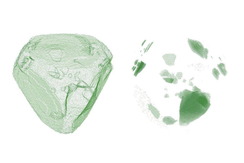
This is where the MUNDFAB project comes in: In order to optimize modeling for an accurate prediction of the processing of, e.g., silicon or silicon-germanium layers used for nano-sized devices, dedicated experiments are carried out to improve the simulation models. For the simulations, the researchers use commercial software tools, open-source applications as well as simulation programs provided by the project partners, which are adapted and further developed in the project. Simulators that can directly represent the atomistic structure of the systems under consideration (the figure shows an example) allow a particularly realistic modeling of the nanostructures. The final goal of the project is to establish a completely calibrated simulation toolchain, which allows the computer-based virtualization of the manufacturing and sequential 3D integration of nano-sized devices.
In February, the project coordinator Fraunhofer IISB hosted the kick-off meeting with all partners. After this meeting, which could still be held as a face-to-face event, it was necessary to switch to virtual collaboration in the following months. For an effective communication and cooperation, the partners used various tools. The results are impressive: Four scientific papers from the project were already be presented at SISPAD 2020, the world’s leading conference on the simulation of semiconductor devices and processes. This year, the conference was all-virtual and took take place from September 23 to October 6. Details are available on the MUNDFAB website (see below) under "Events".
MUNDFAB runs from January 2020 to December 2022 and receives funding within the European Union’s Horizon 2020 research and innovation programme under grant agreement No. 871813 of 3.8 million Euros. The project partners are Fraunhofer IISB (coordinator), CEA-Leti (France), CNR-IMM (Italy), CNRS-LAAS (France), Lukasiewicz-ITME (Poland), STMicroelectronics (France) and TU Vienna (Austria).
Further information, such as publications or technical project reports, is available on the website: https://www.mundfab.eu/
As one of the 74 institutes and research units of the Fraunhofer-Gesellschaft, the Fraunhofer Institute for Integrated Systems and Device Technology IISB conducts contract research for industry and public authorities. Its main objective is to provide excellent research to its customers and to set technological benchmarks as one of the leading research institutions in electronic systems. For this, about 250 employees plus numerous students work on a broad range of power electronics for mobility, industry, and energy supply, semiconductor devices and technology, packaging and modules, and materials development. This is supplemented by broad activities in test and reliability, simulation, characterization, and metrology.
In addition to silicon technology, the IISB has a strong focus on wide-bandgap semiconductors, especially silicon carbide (SiC). For SiC, the institute offers a complete technology backbone, including materials science, devices, modules, and their integration in highly efficient power electronic systems.
Besides its headquarters in Erlangen, Fraunhofer IISB has branches in Nuremberg and Freiberg / Saxony. The institute closely cooperates with the Friedrich-Alexander-Universität Erlangen-Nürnberg (FAU) and is a foundation member of the “Energie Campus Nürnberg” (EnCN) as well as the “Leistungszentrum Elektroniksysteme” (LZE). IISB pursues cooperation with numerous national and international partners in joint projects and associations.
Fraunhofer-Institut für Integrierte Systeme und Bauelementetechnologie IISB
Schottkystraße 10
91058 Erlangen
Telefon: +49 (9131) 761-0
Telefax: +49 (9131) 761-390
http://www.iisb.fraunhofer.de
Telefon: +49 (9131) 761-227
Fax: +49 (9131) 761-212
E-Mail: peter.pichler@iisb.fraunhofer.de
![]()


