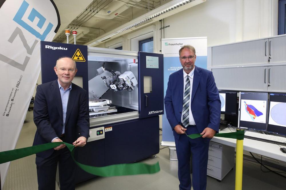
Newly developed, unique XRT tool to revolutionize semiconductor material defect characterization techniques
A newly developed X-ray topography tool was installed at IISB to investigate especially high X-ray absorbing semiconductor materials like GaN, GaAs, InP, CdTe as well as very thin layers obtained by epitaxial processes, e.g. SiC and Nitrides in terms of crystallographic defects. In order to support semiconductor industry worldwide in improving semiconductor materials and device production, Rigaku Cooporation Japan, Rigaku Europe SE and Fraunhofer IISB in Erlangen are pleased to announce the formation of the Center of Expertise for X-ray Topography worldwide, located in Erlangen, Germany.
Dr. Michael Hippler, president at Rigaku Europe SE in Neu-Isenburg, Germany, states: “We are proud to join forces with the highly experienced team at IISB for semiconductor substrate and epilayer characterization by inaugurating the Center of Expertise for X-Ray Topography at Fraunhofer IISB. The newest generation X-ray tool, which we developed together with Fraunhofer IISB will be a milestone for semiconductor material characterization worldwide and a breakthrough for Rigaku Cooperation which will significantly increase the tool portfolio which Rigaku can offer to semiconductor customers worldwide.”
Two different X-ray sources in one tool – silver and chromium – in combination with the application of a large angle goniometer accommodates a wide range of diffraction conditions for different semiconducting materials. On the one hand, this XRT tool development now enables investigation of crystallographic defects with high speed and highest resolution on full wafer scale especially for high X-ray absorbing semiconducting materials like GaN, GaAs, InP, CdTe. On the other hand, the new XRT tool offers the possibility to investigate very thin layers obtained by epitaxial processes, especially dedicated to SiC and Nitrides.
The latest X-ray topography tool is well suited for bare wafers, wafers with epilayer structures, partially processed wafers, as well as bonded wafers. The amount and different types of dislocations, slip lines, dislocation networks, (small angle) grain boundaries, inclusions, precipitates, pits, scratches, stress level, etc. can be imaged and quantified on the samples.
The XRTmicron system can be operated in transmission as well as in reflection mode in order to detect defects in the volume of the sample or to quantify defects close to the surface. Furthermore, it is equipped with a standard and a high resolution XTOP CCD-camera. This leads to a spatial resolution of 5.4 µm and 2.4 µm per pixel, respectively, for a single image size of 18 mm x 13.5 mm. Full wafer mappings and detailed defect imaging of regions of interest are possible under different diffraction conditions for sample sizes of up to 300 mm in diameter.
Additionally, the XRTmicron system is equipped with a special slit-arrangement to perform cross section topography measurements in high resolution. This gives detailed depth information through the whole thickness of the sample. For instance, the defect formation due to epilayer growth on top of a wafer can be quantified by this feature.
Prof. Dr. Martin März, Head of Fraunhofer IISB, states: “We are happy that we have gained Rigaku as one of the largest players in the field of semiconductor material characterization, as a strategic partner in the field of X-ray topography. We are convinced we will up a long-term success story satisfying the needs of semiconductor industry. On the one hand we want to support them with profound scientific knowledge on defect characterization and on the other hand we want to develop industrial applicable measurement routines and defect counting algorithms which can be used in production and for R&D purposes.”
Fraunhofer IISB will act as a demo center for the newest XRTmicron system worldwide. Dr. Martin Fehrentz, Business Development at Rigaku Europe SE, adds, “We already received numerous requests from the semiconductor industry aiming to close the existing gap for structural characterization for semiconducting materials, especially for high X-ray absorbing materials and thin epitaxial layers.” It is therefore planned to standardize the operation procedures for the different costumers due to their specific needs within the strategic collaboration between Rigaku and Fraunhofer IISB.
Dr. Christian Reimann, Group Manager at Fraunhofer IISB and responsible for the XRT business field, adds: ”The common X-ray tool development is the logical next step to revolutionize the semiconductor material defect characterization techniques, which can be used under industrial boundary conditions. The already existing collaboration between IISB and Rigaku since 2019 now bears the first peak of success by installing the Center of Expertise for X-ray topography at IISB.”
About Fraunhofer IISB
Intelligent Power Electronic Systems and Technologies – according to this motto, the Fraunhofer Institute for Integrated Systems and Device Technology IISB, founded in 1985, conducts applied research and development for the direct benefit of industry and society. With scientific expertise and comprehensive systems know-how, IISB supports customers and partners worldwide in transferring current research results into competitive products, for example for electric vehicles, aviation, production, and energy supply.
The institute consolidates its activities in the two major business areas of Power Electronic Systems and Semiconductors. In doing so, it comprehensively covers the entire value chain from basic materials to semiconductor device, process, and module technologies to complete electronics and energy systems. As a unique European competence center for the semiconductor material silicon carbide (SiC), IISB is a pioneer in the development of highly efficient power electronics even for the most extreme requirements. With its solutions, IISB repeatedly sets benchmarks in energy efficiency and performance. By integrating intelligent data-based functionalities, new use cases are continuously emerging.
The IISB employs about 300 people. Its headquarters are in Erlangen, with additional branches at the Energie Campus Nürnberg (EnCN) and the Fraunhofer Technology Center High Performance Materials (THM) in Freiberg. The institute closely cooperates with Friedrich-Alexander-Universität Erlangen-Nürnberg (FAU) and is a founding member of the EnCN as well as the Leistungszentrum Elektroniksysteme (LZE). In joint projects and associations, IISB collaborates with numerous national and international partners.
About Rigaku
Since its inception in Japan in 1951, Rigaku has been at the forefront of analytical and industrial instrumentation technology. Rigaku and its subsidiaries form a global group focused on general-purpose analytical instrumentation and the life sciences. With hundreds of major innovations to their credit, Rigaku companies are world leaders in X-ray spectrometry, diffraction, and optics, as well as small molecule and protein crystallography and semiconductor metrology. Today, Rigaku employs over 1,400 people in the manufacturing and support of its analytical equipment, which is used in more than 90 countries around the world supporting research, development, and quality assurance activities. Throughout the world, Rigaku continuously promotes partnerships, dialog, and innovation within the global scientific and industrial communities.
Fraunhofer-Institut für Integrierte Systeme und Bauelementetechnologie IISB
Schottkystraße 10
91058 Erlangen
Telefon: +49 (9131) 761-0
Telefax: +49 (9131) 761-390
http://www.iisb.fraunhofer.de
Gruppenleiter Silizium
Telefon: +49 (9131) 761-272
Fax: +49 (9131) 761-280
E-Mail: christian.reimann@iisb.fraunhofer.de
![]()


