Pac Tech – Packaging Technologies GmbH Appoints New Vice Presidents to Lead Business Units
Dr. Thorsten Teutsch, CEO of PacTech, expressed his vision for the company’s future, stating, “Our intent is to strengthen our engineering leverage through 2024, enhancing middle management and leadership across all business units and sites. We are incredibly proud to recognize the exceptional talents of Sy Jiun and Matthias, who have been cultivated within PacTech. This decision reflects our commitment to nurturing and advancing internal talent to drive our strategic initiatives forward.”
Ms. Sim began her journey with PacTech as a Customer Support Manager at the Penang subcon site in 2010, subsequently transitioning to PacTech’s headquarters in Germany as Marketing Manager in 2017. With a master’s degree in project management, Ms. Sim will now lead PacTech’s Wafer Level Packaging business units in Southeast Asia and Germany, overseeing the expansion and ramp-up of WLP services utilizing cutting-edge electroless and electroplating process technologies.
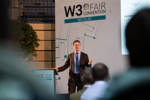
Mr. Fettke, who holds a master’s degree in Laser & Opto-Technology with a specialization in laser material processing, has been instrumental in innovating new laser bonding and soldering technologies at PacTech. He possesses a broad skill set that includes research and development, manufacturing, and product management in the photonics and semiconductor industries. His contributions have led to numerous publications and patents. In his new role as Vice President of Advanced Packaging Equipment, Mr. Fettke will lead the equipment business unit to further advance PacTech’s technological capabilities.
About PacTech
PacTech is a global leader in advanced wafer bumping, packaging, and solder ball placement equipment. The SB2 solder jetting equipment offers unique flux-less and contact-less soldering solutions for camera modules, THT, HDD, and other advanced packaging applications. The Laplace machine platform provides laser automated bonding and reflow solutions along the heterogeneous integration roadmap for packaging of thermally or geometrically challenged semiconductor chips. Additionally, the PacLine series offers high-performance, electroless plating batch systems for fully automated processing of ≥ 300mm wafers. PacTech caters to various markets, including compound semiconductor, photonics, power, 5G, microLED, and MEMS.
PacTech also provides plating chemistries and high-volume subcontractor bumping and die prep services from its manufacturing facilities in Germany (HQ), the USA, and Malaysia.
PacTech is a technology-focused company specialized in advanced packaging equipment manufacturing and wafer level packaging services. Since our establishment, our team has been working relentlessly on developing new leading-edge technologies for the next generation applications. We are known to be highly adaptive to customization and unique applications. Our team of technical experts is striving to resolve various packaging challenges faced by the industry to provide our customers and partners more competitive solutions in terms of cost, time-to-market, and technology advancement. Our headquarter is located in Nauen, Germany with two operation and manufacturing sites in Santa Clara, CA, USA and Penang, Malaysia. Together with our sales and field service teams across the globe, we can cater to the demand within your region.
Pac Tech – Packaging Technologies GmbH
Am Schlangenhorst 7 – 9
14641 Nauen
Telefon: 033214495122
Telefax: +49 (3321) 4495110
https://www.pactech.com
Onlime Marketing Manager
E-Mail: balzer@pactech.de
![]()


