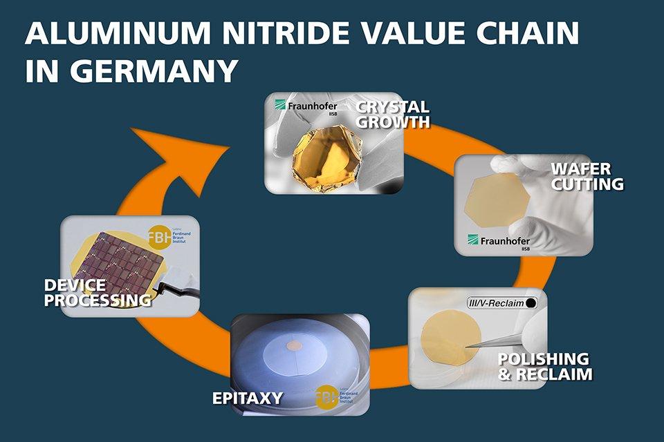
Supply chain for power electronic devices based on novel semiconductor material aluminum nitride – made in Germany
Pole Position for Aluminum Nitride
A new semiconductor technology based on aluminum nitride (AlN) for power electronic transistors as well as millimeter-wave radio-frequency circuits has the potential to significantly reduce losses in electrical energy conversion and high frequency transmission. In power electronics, conventional silicon devices are currently being replaced by more powerful semiconductors with a wide band gap (WBG), i.e. with superior physical and electrical properties. On an industrial scale, silicon carbide (SiC) has already established itself, but devices based on gallium nitride (GaN) are also on the rise. However, it is already foreseeable that even WBG device properties will be surpassed by semiconductors with an ultra-wide band gap (UWBG) in the future. One promising UWBG semiconductor is AlN. Devices on single-crystal AlN wafers reach a higher power density and efficiency compared to GaN technology. They also show lower dynamic parasitic effects and a higher reliability. At the same time, the high thermal conductivity of AlN enables good heat dissipation of the devices.
With the Aluminum Nitride Process Chain to a Leading International Position
In order to make AlN technology accessible to industry in the medium term, the related existing activities in Germany have been combined in a strategic cluster. The aim is to establish a German value chain for AlN-based technology and to build up an international leadership position in this increasingly economically important field. The Ferdinand-Braun-Institut (FBH), the Fraunhofer Institute for Integrated Systems and Device Technology IISB and the company III/V-Reclaim PT GmbH drive this initiative together. They cover the entire value chain, starting with the growth of AlN crystals using the Physical Vapor Transport (PVT) process, to wafering and polishing of epi-ready AlN-wafers, and the epitaxy of the functional device layers, up to the fabrication of transistors for power electronics and millimeter-wave applications.
For the first time, the consortium has now successfully demonstrated the practical implementation of a value chain for AlN devices in Germany and Europe. To this end, AlN crystals were grown at Fraunhofer IISB and sliced into AlN wafers with a diameter up to 1.5 inches. The company III/V-Reclaim has developed a polishing process for epitaxial wafer production. Functional epitaxial layers were then applied to these wafers at the Ferdinand-Braun-Institut, and AlN/GaN high electron mobility transistors (HEMTs) were successfully processed on them. The first transistor generations produced with these wafers already show promising electrical properties, such as a breakdown voltage of up to 2200 V and a power density superior to SiC as well as GaN-based power-switching devices
Investment into and for the Future
Targeting ever higher energy efficiency and progressive miniaturization is crucial for power electronic systems and in microwave communication. However, the static and dynamic conduction losses in the semiconductor materials unnecessarily increase the switching losses in supply, distribution, and usage of electrical energy. This results in a higher consumption of precious primary energy. In Europe alone, conversion losses waste several terawatt hours of electrical energy every year – with a rising trend.
To achieve significant energy savings, the semiconductor material itself must be addressed. Compared to established silicon devices, AlN/GaN HEMTs, as they have now been successfully produced on AlN wafers, offer up to three thousand times less conduction losses than with silicon and are around ten times more efficient than SiC transistors.
These research breakthroughs were supported by funding from the German Federal Ministry of Education and Research (BMBF) within the ForMikro-LeitBAN and Nitrides-4-6G projects.
The Fraunhofer Institute for Integrated Systems and Device Technology IISB is one of Europe’s leading research institutions for wide-bandgap semiconductors and power electronics, covering the complete value chain. The spectrum ranges from basic materials, semiconductor devices and process technologies, power electronic modules and components to complete power electronic and energy systems.
Main target applications of the IISB are semiconductor manufacturing, electromobility, aerospace as well as sustainable energy supply. With its solutions, the institute has been setting benchmarks in energy efficiency and performance, even for extreme operating conditions. The integration of intelligent data-based functionalities also continuously opens up new application scenarios.
Fraunhofer IISB supports its customers and partners worldwide in transferring scientific results into commercial products. Its activities are organized in two business areas: Semiconductor Technology and Power Electronic Systems. A total of around 300 employees works at the headquarters in Erlangen, Bavaria, and at the Fraunhofer Technology Center High Performance Materials THM in Freiberg, Saxony.
Fraunhofer-Institut für Integrierte Systeme und Bauelementetechnologie IISB
Schottkystraße 10
91058 Erlangen
Telefon: +49 (9131) 761-0
Telefax: +49 (9131) 761-390
http://www.iisb.fraunhofer.de
Group Manager Nitride Materials
Telefon: +49 9131 761 182
E-Mail: sven.besendoerfer@iisb.fraunhofer.de
![]()
Das könnte dich ebenfalls interessieren
Swiss Steel Group zählt zu den Weltmarktführern im Langstahl und Spezialprodukte-Bereich
Luftultraschall zur Prozess- und Qualitätsüberwachung in der Polymerschaumextrusion