X-FAB adds CMOS integration option to its galvanic isolation solution
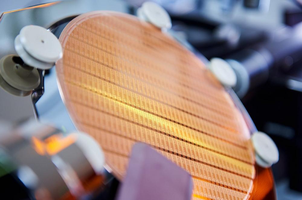
Based on a 350nm process node, XA035 is highly suited to the fabrication of automotive sensors and high-voltage industrial devices. The high-voltage signal isolation capabilities it now supports mean long-term operational performance is maintained, even in demanding environments. It will enable the manufacture of robust components that are AEC-Q100 Grade 0 compliant and industrial-rated, such as digital isolators, isolated gate drivers, and isolated amplifier ICs. X-FAB provides a comprehensive PDK that supports the new and improved process technology for all major EDA vendors.
“We see a growing demand from our customers for robust foundry solutions to design galvanically isolated products. X-FAB has been in production for several years with its proven high-reliable isolation layer for discrete coupler implementations,” states Tilman Metzger, Marketing Manager for High-Voltage Products at X-FAB. “By leveraging the very same process module, we are now able to offer even more flexibility in designing such products by enabling the direct integration with CMOS circuits on the same die. We are also excited to see the first integrated customer products nearing production.”
Acronyms
CMOS – Complementary metal-oxide-semiconductor
EDA – Electronic Design Automation
EV – Electric Vehicle
IC – Integrated Circuit
PDK – Process Design Kit
X-FAB is the leading analog/mixed-signal and MEMS foundry group manufacturing silicon wafers for automotive, industrial, consumer, medical and other applications. Its customers worldwide benefit from the highest quality standards, manufacturing excellence and innovative solutions by using X-FAB’s modular CMOS and SOI processes in geometries ranging from 1.0 µm to 130 nm, and its special silicon carbide and MEMS long-lifetime processes. X-FAB’s analog-digital integrated circuits (mixed-signal ICs), sensors and micro-electro-mechanical systems (MEMS) are manufactured at six production facilities in Germany, France, Malaysia and the U.S. X-FAB employs more than 4,200 people worldwide. Learn more at xfab.com.
X-FAB Semiconductor Foundries AG
Haarbergstrasse 67
99097 Erfurt
Telefon: +49 (361) 427-6000
Telefax: +49 (361) 427-6111
http://www.xfab.com
MarCom
Telefon: +49 (361) 427-6162
E-Mail: anja.noack@xfab.com
![]()


