Processes and technological challenges for low-pressure MEMS sensors
Pressure sensors measure pressure differences. Depending on the application, the difference between two process pressures may be of interest. However, a process pressure is often also measured relative to the atmospheric pressure. The atmospheric pressure varies slightly depending on different parameters such as geographical position and weather, but in many situations this is negligible or even has a stabilising effect on the process. If a constant reference pressure is required, the absolute vacuum is used as a reference in most cases. This is the case with barometers, for example, which can be used to measure changes in atmospheric pressure in absolute terms.
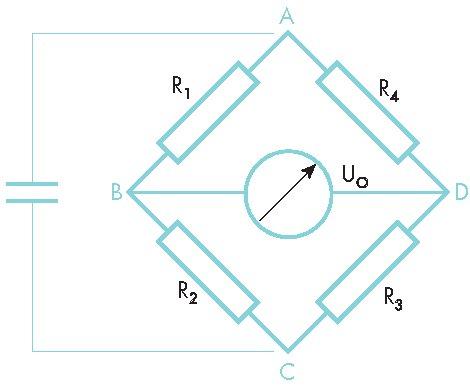
In the vast majority of cases, a diaphragm is used to measure these pressure differences. This can be made from a wide variety of materials such as steel, ceramic or silicon. The pressure difference leads to a deflection of this diaphragm, the magnitude of which must in turn be measured. If the the properties and the deflection of a diaphragm are known, the pressure difference can be derived from this. A common method of measuring the deflection is to use resistors that change their value due to the deflection of the diaphragm. The Wheatstone bridge can be used to reliably convert slight changes in the resistance value of several resistors into a voltage signal. In this arrangement, R1 and R2 form one voltage divider, R3 and R4 the other. The difference between the output voltages of the two voltage dividers corresponds to the output signal of the entire measuring bridge. The resistors are then arranged in such a way that R1 and R3 reduce their resistance value when diaphragm deflects due to pressurisation and R2 and R4 increase theirs. The bridge is supplied via an electrical voltage between A and C. If the sensor is now pressurised, this results in an increaed voltage at B and a decreased voltage at D, and therefore a positive output voltage between B and D.
With a completely unloaded membrane, an output signal of 0mV is aimed for in most cases, i.e. R1=R2=R3=R4=R. As an example, this value R is set at 3500 ohms, while the supply voltage is 5V. This means that the voltages of B and D are both at 2.5V. Under maximum load, the resistance difference is 30 ohms, i.e. R1=R3=3530, R2=R4= 3470. The level at B thus rises to 2.521 V, at D it falls to 2.479 V. This results in an output signal of 42.1mV between B and D at maximum pressurisation. This signal can then be amplified and further conditioned to achieve maximum accuracy.
In piezoresistive MEMS pressure sensors, the diaphragm is made of silicon. The most important parameters of the diaphragm are its surface area and thickness. Larger and thinner diaphragms are generally required to measure smaller pressure differences.
As the name suggests, the deflection is measured using piezoresistors. Piezoresistors are characterised by the fact that they change their resistance under mechanical stress. Such piezoresistors are placed at the perimeter of the diaphragm, where the mechanical stress is greatest due to the difference in stiffness between the diaphragm and the frame around the diaphragm. In the context of pressure sensor diaphragms, the mechanical stress that occurs is always a tensile stress. But, depending on whether a piezoresistor is arranged parallel or perpendicular to the edge of the diaphragm, this tensile stress results in either a reduced or increased resistance. This can be illustrated analogous to the influence of the geometry of a conductor on its electrical resistance. The mechanical tensile stress exerted on a piezoresistor arranged parallel to the edge of the diaphragm corresponds to an ‘increase’ in the conductor cross-section and thus a reduction in resistance. With a piezoresistor arranged perpendicularly, on the other hand, the mechanical tensile stress corresponds to an ‘extension’ of the conductor and is thus accompanied by an increase in resistance. It is important to emphasise that this analogy only serves to illustrate the piezoelectric effect. The piezoresistors do not deform.
From the raw wafer to the MEMS chip
A large proportion of the processes used to manufacture MEMS components come from the traditional semiconductor industry. These are essentially different processes for material deposition, photolithography, ion implantation and etching. Various cleaning processes are also used to remove particles, reaction products and other substances from the wafers. The etching processes in particular involve additional processes that are only used in the production of MEMS components.
A key MEMS process is the deposition of thin films on the wafer. This allows different materials to be applied to the wafer. These can be metals, for example, which are used to create electrical connections on the chip. One example of deposition processes is chemical vapour deposition. Here, reactive gases are diffused onto the wafer and absorbed by it. This is followed by a reaction on the wafer surface in which the desired material precipitates in a solid phase and is deposited as a thin layer of 1-10 nm on the wafer surface. By-products of the chemical reaction are desorbed and transported away from the wafer.
To gain functionality from these deposited layers, they must be structured. This is done through selective etching, which is in turn enabled by photolithography. To do this, a photoresist is first applied to the wafer, often by means of spin coating. This is then selectively exposed through an optical mask. This exposure changes the chemical properties of the resist in such a way that only the chemically altered regions of the resist can be removed in the next step, in the case of positive resist, or only the unaltered regions of the resist can be removed in the case of negative resist.
As a result, defined areas of the wafer are exposed by the optical mask, while other areas are protected by photoresist. This condition can be used to selectively process these exposed regions of the wafer, for example by etching or ion implantation.
In ion implantation, non-silicon atoms are doped into the surface of the wafer. To do this, ions are accelerated onto the wafer in a high vacuum. In most cases, the wafer is masked before this step in order to introduce these foreign atoms only locally. These atoms usually manipulate the electrical properties of the doped material. For example, the conductivity of silicon can be altered to produce a defined resistance. The piezo resistors essential for the pressure sensor, which measure the voltage of the membrane, are produced in this way.
A masked wafer can also be selectively etched. The etching processes are essentially divided into wet etching processes, in which liquid etching solutions are used, and dry etching processes, in which etching is carried out using plasma. Etching steps are typically used to structure materials on the wafer or to remove auxiliary layers. During structuring, the areas of a thin film that are not protected by photoresist are etched away.
After structuring the auxiliary layer, the photoresist must be etched away. In both of these steps, etch selectivity is of great importance. For example, let’s say an aluminium layer was applied directly to a silicon wafer using vapour deposition. The aluminium layer has been masked with photoresist using photolithography. In order to structure the aluminium layer, an etching medium is required that attacks the aluminium much more strongly than the photoresist and the silicon, as the photoresist should protect the regions of the aluminium layer to be preserved and the silicon under the aluminium should not be attacked. When etching away the photoresist, an other etching medium is desired that attacks the photoresist much more strongly than the now exposed silicon and the aluminium that comes to light under the photoresist during the etching step.
Deep reactive ion etching (DRIE) is an advanced etching process that is used to etch deep structures as orthogonally as possible into the wafer substrate. In the first step, the wafer is masked so that only the regions to be etched are exposed. The first etching step then begins. For this, ions from an SF6 plasma are accelerated in an electric field. This primarily removes material orthogonally to the wafer surface. However, as this etching step does not progress 100% orthogonally, the etching step is stopped after a short time and a passivation layer is applied over the entire wafer. Then etching continous as before, first etching away the passivation layer on the bottom of the trench and then etching the trench deeper.
These two steps are repeated alternatingly until the desired trench depth is reached. The result is a microstructure with walls that are largely orthogonal to the wafer surface. These have a characteristic wavy surface.
In the context of pressure sensors, the DRIE method has advantages and disadvantages compared to classic wet etching with potassium hydroxide (KOH):
With DRIE, each wafer has to be processed individually, which leads to higher cost per wafer than with wet etching, where entire wafer lots can be etched at the same time.
Furthermore, the size of the entire chip can be reduced while maintaining the same membrane size due to the vertical walls under the membrane produced using DRIE, which leads to lower costs per chip.
One disadvantage of KOH is that wet-etched structures must be rectangular, as KOH etches anisotropically, whereas DRIE allows orthogonal etching of any geometry. With an adapted geometry, for example, the mechanical stress concentration can be optimised.
Another advantage of DRIE etching, which is particularly important for low-pressure sensors, is the nature of the etch stop. In the case of a pressure sensor, this is the back of the membrane. With KOH etched products, this etch stop is uneven. With DRIE, a significantly less uneven surface can be produced. The flatness of the back of the diaphragm is particularly important for low-pressure sensors, as the diaphragm is particularly thin. The same amount of unevenness results in a significantly greater deviation from the nominal thickness on a thinner diaphragm.
Absolute or differential?
Depending on the application, absolute, relative or differential pressure measurement may be of interest. For absolute pressure sensors, a vacuum must be generated and maintained on one side of the membrane, which is most easily achieved by wafer bonding.
During wafer bonding, two separate wafers are fused together. In the case of MEMS pressure sensors, one wafer is a silicon wafer as described above. The other wafer can also be a silicon wafer, but more often it is a glass wafer. There are different wafer bonding processes, with anodic bonding being the most common for MEMS pressure sensors. The two polished and treated wafers form a strong bond under temperature and electrical voltage.
Wafer bonding can be used to manufacture absolute pressure sensors. To do this, the pressure on one side of the membrane must be kept constant. This is achieved by bonding a glass wafer to the back of a MEMS pressure sensor wafer in a vacuum environment. This allows any pressure applied from the front to be measured relative to the vacuum prevailing on the back of the diaphragm and thus in absolute terms.
From MEMS chip to pressure sensor
Piezoresistive MEMS pressure sensors convert a mechanical voltage into an electrical signal. In order to obtain a signal that is as accurate as possible, the converted mechanical voltage should be caused exclusively by the applied pressure. The influence of other sources of mechanical stress should therefore be minimised.
The most significant source of such undesirable stresses is temperature. As every material has a different thermal expansion, temperature changes lead to uneven expansion or contraction, which in turn leads to mechanical stresses. These effects are naturally taken into account when designing a MEMS chip. For example, critical structures are constructed as symmetrically as possible to prevent a bimetallic-style bending effect. Where possible, however, materials with similar thermal properties are chosen from the get go.
It is not only important to consider such effects when designing the chip. Attention must also be paid to the mechanical connection between the pressure chip and the housing of a pressure sensor, known as the die attach. Depending on the housing material, the
difference in thermal expansion between chip and housing is considerable. For example, if a silicon chip with a thermal expansion of 2.56×10⁻⁶/K is mounted directly in a plastic housing with a thermal expansion of 26×10-6/K, significant voltages are transferred to the chip when the temperature changes.
The lower the nominal pressure measuring range of the chip, the more sensitive the chip is to such stresses. It is therefore advisable to carry out tests with different adhesives, especially when mounting low-pressure chips. The different methods of applying the adhesive should also be evaluated.
The most important properties of the die attach are its hardness, the distance between the silicon chip and the housing and the contamination of the chip walls. In terms of hardness, the die attach should be as soft as possible, as this allows it to absorb as much stress as possible. The distance between the chip and the housing should be sufficiently large, again to enable the absorption of stresses. However, the die attach should move up the walls of the silicon chip as little as possible, as this in turn reduces decoupling.
To simplify the task of the die attach, a back glass can be implemented on the sensor chips. This is done similarly to absolute pressure sensors by means of wafer bonding. Glass has a relatively similar thermal expansion to silicon (3.2×10⁻⁶/K vs. 2.56×10⁻⁶/K). This results in minimal temperature-related stress between glass and silicon, while the glass can largely absorb stresses coming from the sensor housing. This can massively simplify the die attach process, as such a chip with backside glass can be bonded quite easily.
However, glass has the disadvantage that it is an amorphous material. In contrast to silicon, glass is therefore not crystalline, which means that glass can change geometrically or ‘flow’ in the long term. This involves periods of months and years over which the glass changes, causing mechanical stress in the silicon chip. This is then visible in the sensor signal as zero-offset drift. This effect is particularly noticeable with low-pressure sensors, whereas it is usually negligible at higher pressure ranged chips. For the best long-term low-pressure performance, a silicon chip attached using a well-implemented die attach process is therefore preferable to a chip with backside glass.
Which sensor design and technology is best for the DIE attachment depends on the application. This can vary depending on the application, medium and pressure range. All these factors must be considered in order to design and produce the best sensor for a particular application.
Personal consultation, fast reaction times and customised solutions have set Angst+Pfister Sensors and Power apart for close to 30 years.
Our broad and deep range of sensors, power supplies and electronic components ensures you find the right components for your particular field of application. Depending on your requirements, we deliver to our customer standard products, modified standard products or customised solutions. We work exclusively with selected and proven partners that share our uncompromising commitment to reliability, durability, value for money and quality. In addition, the production and distribution of Angst+Pfister Sensors and Power own products complement our broad portfolio.
We do not leave our customers alone during the development phase, but always seek the best solution for your application. Our specialists have deep technical understanding and will accompany through the whole process.
Angst+Pfister Sensors and Power is a daughter company of the Angst+Pfister Group and serves customers across Europe and the globe. We are part of a worldwide network with more than 1 000 employees and 60 000 satisfied customers. With the acquisition of IS-LINE via the Angst+Pfister group, we are able to generate further added value for our clients through expert technical advice and an even broader portfolio in the field of sensors and power electronics. Together we are part of a worldwide network with more than 1,000 employees and 60,000 satisfied customers.
Angst+Pfister Sensors and Power AG
Thurgauerstrasse 66
CH8050 Zürich
Telefon: +41 (44) 87735-00
Telefax: +41 (44) 87735-25
http://sensorsandpower.angst-pfister.com
Marketing Manager
Telefon: +41 (44) 877 35 26
Fax: +41 (44) 8773525
E-Mail: yun.xu@angst-pfister.com
![]()


