Advantest Introduces Latest Image-Processing Engine for Testing CIS Devices Used in High-Resolution Smart Phones
Smart phone applications, the largest end-use application for CIS devices, are forecast to grow to $15.7 billion in 2025, according to market research firm IC Insights. While the number of cameras in smart phones is increasing, so is the pixel count per camera. Currently available CIS devices within today’s most advanced smart phones incorporate more than 100 million pixels to achieve high resolution. Also, the CIS market is expected to grow at a CAGR of 14.9 percent from 6.7 billion units in 2020 to 13.5 billion units by 2025.
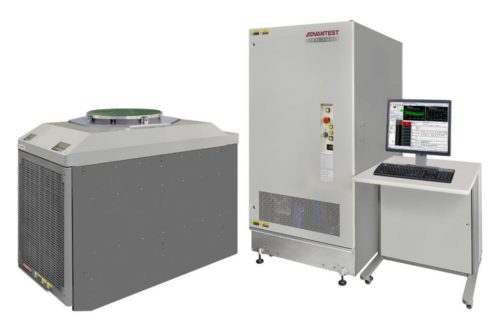
The new T2000 IP Engine 4 features enhanced computing power to handle huge volumes of imaging data while also reducing test times and the cost of test. Used along with Advantest’s 4.8GICAP image capture module, the new tester can perform high-volume, at-speed testing of the most advanced mobile CIS including 3.5-Gsps C-PHY and 4.8-Gbps D-PHY devices. Image-processing accelerators enable fast testing of high-resolution CIS with more than 200 million pixels.
The system is supported by a dedicated image-processing library optimized for the IP Engine 4. The algorithms provided are suitable for high-speed image-processing environments, helping to facilitate test program development.
Designed for installation on the T2000 ISS platform, the IP Engine 4 is fully compatible with previous generations of image-processing engines and is easily upgradable, enabling users to leverage their existing assets including test programs and probe cards.
“Our new IP Engine 4 delivers the industry’s fastest image processing, a key capability in reducing test times and production costs,” said Toshiaki Adachi, vice president of the T2000 Business Unit for Advantest Corporation. “We expect this test solution to play a key role as high-resolution CIS devices spread beyond high-end smart phones into mid-range handsets and other broad consumer market segments.”
The first T2000 IP Engine 4 systems are now being evaluated by Advantest’s strategic partners.
Advantest (TSE: 6857) is the leading manufacturer of automatic test and measurement equipment used in the design and production of semiconductors for applications including 5G communications, the Internet of Things (IoT), autonomous vehicles, artificial intelligence (AI), machine learning, smart medical devices and more. Its leading-edge systems and products are integrated into the most advanced semiconductor production lines in the world. The company also conducts R&D to address emerging testing challenges applications, produces multi-vision metrology scanning electron microscopes essential to photomask manufacturing, and offers groundbreaking 3D imaging and analysis tools. Founded in Tokyo in 1954, Advantest is a global company with facilities around the world and an international commitment to sustainable practices and social responsibility. More information is available at www.advantest.com.
Advantest Europe GmbH
Stefan-George-Ring 2
81929 München
Telefon: +49-89-993-12-0
http://www.advantest.com/
Assistant Managing Director
Telefon: +49 (89) 99312-131
Fax: +49 (89) 99312-108
E-Mail: Claudia.erspamer@advantest.com
![]()


