-
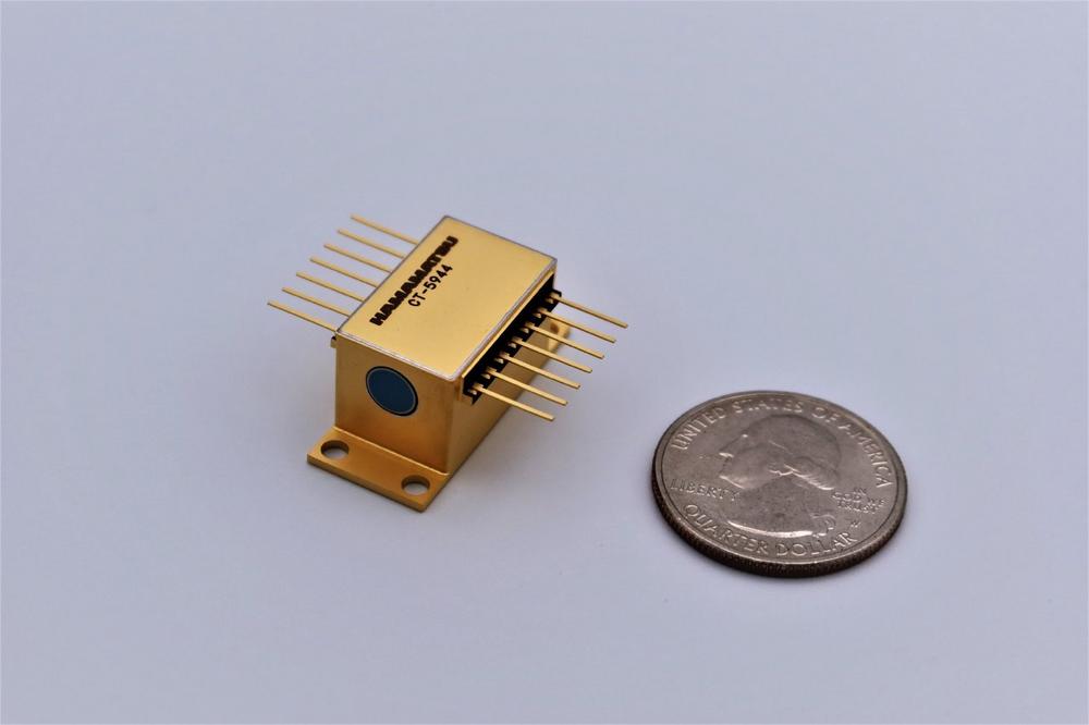
The world’s smallest wavelength-swept quantum cascade laser (QCL) mountable in small spaces as a light source designed for portable volcanic gas monitoring systems
By leveraging our unique micro electromechanical system (MEMS) technology and optical mounting technology, Hamamatsu Photonics have newly designed and developed the world’s smallest wavelength-swept quantum cascade laser (QCL) to a size that is a mere 1/150th that of previous products! This breakthrough stems from the “Development of sensing technology for detecting extremely weak signals to realize an IoT society” project supported by the New Energy and Industrial Technology Development Organization (NEDO), Japan’s largest national research and development agency. Combining this new QCL with a drive system developed by the National Institute of Advanced Industrial Science and Technology (AIST) will help achieve high-speed operation and simplify the peripheral circuit design, allowing…
-
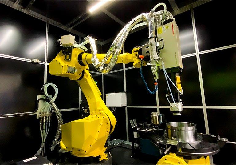
Hamamatsu Photonics has developed laser thermal processing equipment capable of operating with a high degree of freedom while emitting continuous to pulsed irradiation with a minimum pulse width of 4 milliseconds
At Hamamatsu Photonics we have developed laser thermal processing equipment for laser quenching that combines a direct diode laser, (DDL) that we newly designed and developed based on our unique laser diode (LD) technology, with a 6-axis robotic arm capable of operating with a high degree of freedom. This equipment irradiates a laser beam with an output power of 2.5 kilowatts (kW) ideal for surface quenching onto steel materials of various shapes and sizes. It also offers a low running cost which will lead to wider use of laser quenching. The heating temperature can be precisely adjusted by setting the laser irradiation time per shot to any desired time from…
-
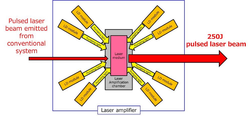
Hamamatsu Photonics develops an industrial pulsed laser system delivering the world’s highest output power of 250 joules!
Hamamatsu Photonics successfully developed an industrial pulsed laser system that produces a pulse energy of 250 J (joules) which is the world’s highest energy among LD-pumped lasers. The development of this laser system stems from the “Research and Development of Next Generation Laser Processing Technology” project supported by the NEDO, which is a national research and development agency in Japan. This new laser system boosts the energy storage capability of the laser medium as well as beam quality to deliver more than double the energy amplification capability while still maintaining the same size as currently available industrial pulsed lasers. Acquiring and integrating the processing-machining data from this laser system will…
-
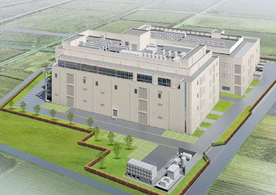
Koso Corporation, a production subsidiary of Hamamatsu Photonics, will be constructing a new factory building to boost its production capacity of electron tube light sources
Koso Corporation (677-1, Kakeshita, Iwata City, Shizuoka Prefecture, Japan) is a subsidiary of Hamamatsu Photonics which manufactures electron tube light sources. Koso Corporation will soon begin construction of a new factory Building No. 2 to boost production capacity. The groundbreaking ceremony for the new factory building will be held on Monday, August 2, 2021 and the new factory building will be completed in July 2022. In 1987, Hamamatsu Photonics established the Koso Corporation as a production subsidiary to handle its ever expanding sales of light sources in the electron tube field. In 2010, the current factory was constructed to consolidate production functions, that up to then had been dispersed in…
-
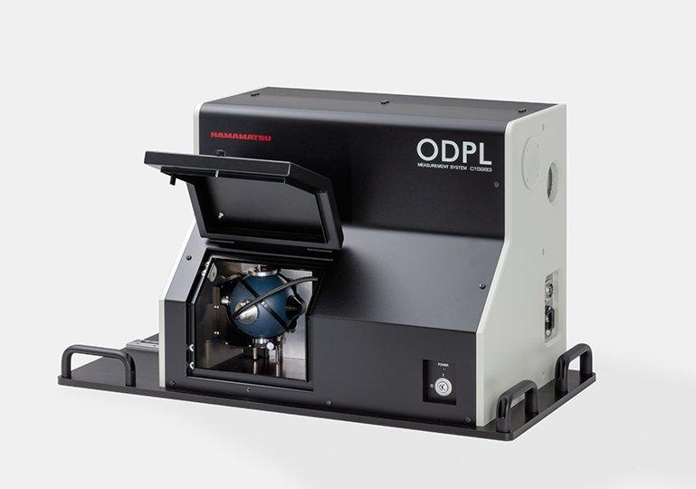
Hamamatsu Photonics has developed a GaN crystal evaluation system that uses ODPL spectroscopy to quantitatively evaluate GaN crystal quality
Hamamatsu Photonics has developed a GaN (gallium nitride) crystal evaluation system “ODPL (omnidirectional photoluminescence) measurement system C15993-01” that leverages ODPL spectroscopy along with our unique light detection technologies including optical design and data processing. This ODPL measurement system quantitatively evaluates the quality of GaN crystals that are currently drawing vast attention as a material for next-generation power semiconductors. This new system will prove a powerful tool for enhancing R&D efficiency to discover new ways to improve crystal quality. Sales of this new ODPL measurement system start on Monday, August 2, 2021 for researchers at universities and semiconductor substrate manufacturers both in Japan and overseas. The system will be presented at…
-
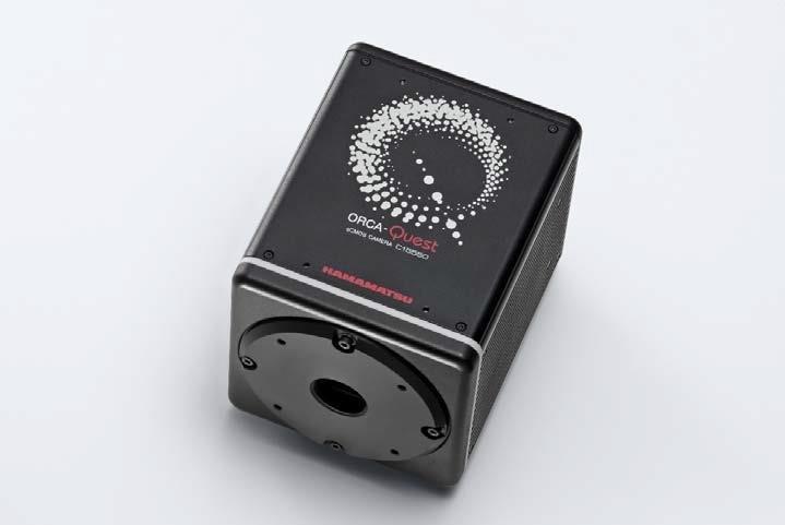
Hamamatsu Photonics introduces the world’s first photon-number-resolving scientific camera with incredibly low noise and 9.4 megapixels
Hamamatsu Photonics has designed and produced a scientific camera called the ORCA®-Quest qCMOSTM camera (part number C15550-20UP), having incredibly low noise of 0.27 electrons rms and a high pixel number of 9.4 megapixels. What makes this possible is a new two-dimensional CMOS (complementary metal-oxide semiconductor) image sensor, designed by applying our unique design technology and fabricated using the latest manufacturing technologies. In quantitative imaging, the photoelectric noise generated when light is converted into electrical signals is the all-important factor that determines the lower detection limit of the camera. The ORCA-Quest reduces this photoelectric noise to a level below the signals generated by photons (particles of light), which are the minimum…
-
Hamamatsu Photonics will construct a new factory building at the Toyooka factory site to boost production capacity of its electron tube products
Hamamatsu Photonics will construct a new factory Building, No. 11, at its Toyooka factory site (Shimokanzo, Iwata City, Japan) to handle the increase in sales of Microfocus X-ray sources (MFX) and other electron tube products. The groundbreaking ceremony for the new factory building will be held on Wednesday 19 May 2021, and is scheduled to be completed in January 2023. At Hamamatsu Photonics we manufacture and sell highly advanced electron tube products such as photomultiplier tubes, imaging devices and light sources for a broad range of fields and applications including medicine, industry, analysis, measurement, and academic research. We see sales of these products steadily increasing, particularly with the rapidly expanding…
-
Hamamatsu Photonics launches a new Webinar: qCMOS
This webinar with Peter Seitz, Ph.D., will provide an overview of semiconductor image sensors and introduce photon-resolving quantitative CMOS imaging (qCMOS). Wednesday, May 19th at 5:00pm CEST, 11:00AM EDT Register: https://www.hamamatsu.com/eu/en/news/event/2021/20210519190000.html About this webinar: Imaging in general and semiconductor imaging in particular have penetrated every aspect of our lives, especially in the sciences. They have empowered many experiments from relying on subjective recording into objectively documentable, repeatable, and quantifiable methods. The evolution of imaging technology is directly linked to new scientific achievements. Demanding and extremely valuable techniques such as single-molecule-based methods would not be possible without appropriate image sensors. Conceptually, all imaging procedures have to find their optimum trade-off between…
-
Hamamatsu Photonics will construct a new factory building at the Joko factory site to boost production capacity of image measurement devices and equipment business
Hamamatsu Photonics will construct a new factory, Building No. 5 at the Joko factory site (Joko-cho, Higashi-ku, Hamamatsu City, Japan) to handle expanding sales of image measurement devices and equipment such as digital cameras for scientific measurement, digital pathology slide scanners, and semiconductor failure analysis systems. The groundbreaking ceremony for the new factory building is scheduled to be held on April 20, 2021, and the new factory building will be completed in June 2022. At Hamamatsu Photonics we develop, manufacture and sell a broad spectrum of image measurement devices and equipment that have high speed, high sensitivity, and high resolution, making them ideal for a range of applications including medical,…
-
Hamamatsu Photonics has developed laser thermal processing equipment capable of operating with a high degree of freedom
At Hamamatsu Photonics we have developed laser thermal processing equipment for laser quenching that combines a direct diode laser, (DDL) that we newly designed and developed based on our unique laser diode (LD) technology, with a 6-axis robotic arm capable of operating with a high degree of freedom. This equipment irradiates a laser beam with an output power of 2.5 kilowatts (kW) ideal for surface quenching onto steel materials of various shapes and sizes. It also offers a low running cost which will lead to wider use of laser quenching. The heating temperature can be precisely adjusted by setting the laser irradiation time per shot to any desired time from…

